The US is tightening restrictions on China’s access to chipmaking gear, two major equipment suppliers have said, underscoring Washington’s accelerating efforts to curb Beijing’s economic ambitions.
Washington had banned the sale of most gear that can fabricate chips of 10 nanometers or better to Chinese firm Semiconductor Manufacturing International Corp (SMIC, 中芯國際) without a license.
Now it has expanded that barrier to equipment that can make anything more advanced than 14 nanometers, Lam Research Corp chief executive officer Tim Archer told analysts.
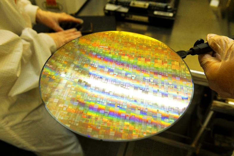
Photo: Bloomberg
The moratorium likely extends beyond SMIC and includes other fabrication plants run by contract chipmakers operating in China, including those by Taiwan Semiconductor Manufacturing Co (TSMC, 台積電).
“We were recently notified that there was to be a broadening of the restrictions of technology shipments to China for fabs that are operating below 14 nanometers,” Archer said during a conference call on Wednesday. “That’s the change, I think, people have been thinking might be coming and we’re prepared to fully comply. We’re working with the US government.”
In chip manufacturing, production identified by lower numbers of nanometers is more advanced. That means raising the restriction level to 14 nanometers would cover a broader range of semiconductor equipment.
The US Department of Commerce said in a statement that the administration of US President Joe Biden is tightening policies aimed at the People’s Republic of China (PRC), without specifying the precise chip geometry.
“The Biden administration is focused on impairing PRC efforts to manufacture advanced semiconductors to address significant national security risks to the United States,” the agency said.
All US equipment makers have in the past few weeks received letters from the commerce department telling them not to supply gear to Chinese firms for manufacturing at 14 nanometers or below, people familiar with the matter said.
The letters are at least partly an effort by the Biden administration to look tough on China, but the department had already declined many licenses at 14 nanometers so the change would have little financial effects, they said.
The new requirements are targeted at foundries — facilities making logic chips for others — and exclude memory chips “to the best of our understanding,” Archer said.
Lam Research executives said they had incorporated the expected effects of the US requirements into their outlook for the third quarter of this year, without elaborating.
KLA Corp CEO Rick Wallace on Thursday confirmed that his company had been notified by the US government of the change in export licensing requirements on China-bound gear for chips more advanced than 14 nanometers.
Wallace said there was no material impact on KLA’s business.
The comments from the two California-based companies mark the first detailed confirmation that the Biden administration is ramping up attempts to contain China. The US is pushing partner countries such as the Netherlands and Japan to ban ASML Holding NV and Nikon Corp from selling mainstream technology essential in making a large chunk of the world’s chips to China.
The new rules cover a wider swath of semiconductors across a plethora of industries and possibly affect far more companies than standing restrictions targeted at SMIC. While the new curbs specifically cover equipment capable of making chips more advanced than 14 nanometers, mature chips could still be affected, as about 90 percent of gear is compatible from one generation to the next. Semiconductor manufacturers can reuse equipment as they migrate to more sophisticated nodes, meaning a ban on one generation could have longer-term ripple effects.
SMIC’s most sophisticated technology is 14 nanometers, while the best TSMC uses in China is 16 nanometers. Those are three generations behind the most cutting-edge technology TSMC uses in Taiwan.
The new rules are likely to affect SMIC, TSMC and any others with the ambition to build capacity for relatively advanced chips in China, as well as gear makers such as Applied Materials Inc, ASML and Tokyo Electron Ltd, which sell to the world’s largest chip market.

MAJOR BENEFICIARY: The company benefits from TSMC’s advanced packaging scarcity, given robust demand for Nvidia AI chips, analysts said ASE Technology Holding Co (ASE, 日月光投控), the world’s biggest chip packaging and testing service provider, yesterday said it is raising its equipment capital expenditure budget by 10 percent this year to expand leading-edge and advanced packing and testing capacity amid strong artificial intelligence (AI) and high-performance computing chip demand. This is on top of the 40 to 50 percent annual increase in its capital spending budget to more than the US$1.7 billion to announced in February. About half of the equipment capital expenditure would be spent on leading-edge and advanced packaging and testing technology, the company said. ASE is considered by analysts

TRANSFORMATION: Taiwan is now home to the largest Google hardware research and development center outside of the US, thanks to the nation’s economic policies President Tsai Ing-wen (蔡英文) yesterday attended an event marking the opening of Google’s second hardware research and development (R&D) office in Taiwan, which was held at New Taipei City’s Banciao District (板橋). This signals Taiwan’s transformation into the world’s largest Google hardware research and development center outside of the US, validating the nation’s economic policy in the past eight years, she said. The “five plus two” innovative industries policy, “six core strategic industries” initiative and infrastructure projects have grown the national industry and established resilient supply chains that withstood the COVID-19 pandemic, Tsai said. Taiwan has improved investment conditions of the domestic economy

Malaysia’s leader yesterday announced plans to build a massive semiconductor design park, aiming to boost the Southeast Asian nation’s role in the global chip industry. A prominent player in the semiconductor industry for decades, Malaysia accounts for an estimated 13 percent of global back-end manufacturing, according to German tech giant Bosch. Now it wants to go beyond production and emerge as a chip design powerhouse too, Malaysian Prime Minister Anwar Ibrahim said. “I am pleased to announce the largest IC (integrated circuit) Design Park in Southeast Asia, that will house world-class anchor tenants and collaborate with global companies such as Arm [Holdings PLC],”

Huawei Technologies Co’s (華為) latest smartphones carry a version of the advanced made-in-China processor it revealed last year, results from an independent analysis showed. This underscored the Chinese company’s ability to sustain production of the controversial chip. The Pura 70 series unveiled last week sports the Kirin 9010 processor, research firm TechInsights found during a teardown of the device. This is a newer version of the Kirin 9000s, made by Semiconductor Manufacturing International Corp (SMIC, 中芯) for the Mate 60 Pro, which had alarmed officials in Washington who thought a 7-nanometer chip was beyond China’s capabilities. Huawei has enjoyed a resurgence since